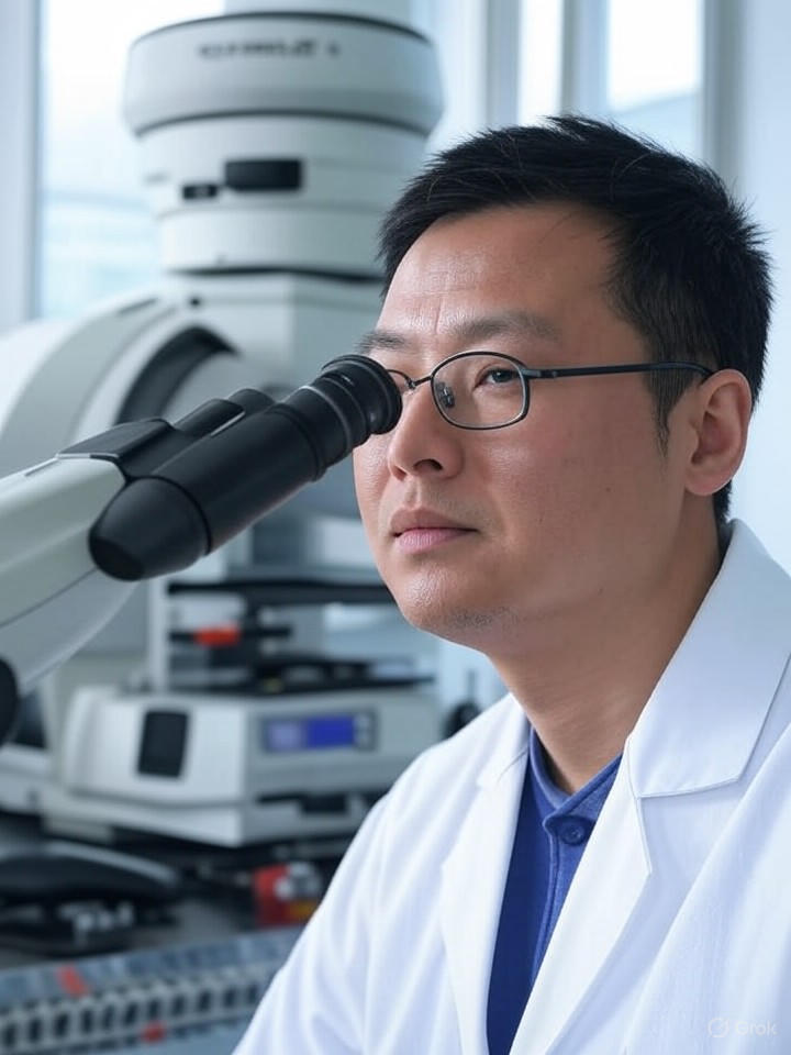
In a significant advancement for semiconductor manufacturing, researchers in China have introduced a novel method that utilizes cryogenic electron tomography (cryo-ET) to dramatically reduce polymer residues during the lithography process by 99%. This breakthrough, detailed in the journal Nature, has the potential to enhance chip yields significantly while lowering production costs.
In the competitive landscape of semiconductor fabrication, even the smallest defects can lead to substantial financial losses. The team”s use of cryo-ET allows for the freezing of photoresist materials at extremely low temperatures, enabling the identification and removal of defects that have historically hindered wafer production. By reconstructing the structure of polymers in liquid films, the researchers were able to identify the sources of imperfections that result in failures of circuit patterns on 12-inch wafers.
This innovative approach represents a major shift in how the semiconductor industry addresses yield challenges, particularly as manufacturers strive for increasingly smaller nodes. The cryo-ET technique provides unprecedented clarity in detecting residual polymers that traditional optical inspections often miss, which can result in yield rates below 90% for advanced nodes. As one analyst noted, “It”s like having X-ray vision for molecular hiccups,” highlighting the method”s precision.
The development of this technique comes at a time when China is making significant investments to enhance its semiconductor capabilities amid stringent U.S. export controls on advanced technologies. The research team has successfully applied the cryo-ET method to processes compatible with existing fabrication techniques, demonstrating its potential for scalability on standard production lines. Initial tests indicate not only a reduction in defects but also possible savings in manufacturing costs through more efficient developer usage.
Comparing this new method to conventional approaches reveals its advantages: while traditional inspections struggle with nanoscale residues, the cryogenic technique achieves nearly flawless lithography by preserving samples in their natural state for detailed analysis. This advancement could accelerate China“s journey toward self-sufficiency in high-end semiconductor production, particularly for nodes of 7nm and below.
Despite its promise, the integration of cryo-ET into high-volume fabs poses challenges, particularly the need for upgrades to cryogenic infrastructure, which could incur initial costs but ultimately lead to reduced waste. The breakthrough stems from real-time reconstruction of polymer behavior, paving the way for defect-free wafers that could rival the capabilities of industry leaders like TSMC and Intel.
Looking beyond immediate applications, this technology could enhance extreme ultraviolet (EUV) lithography for sub-5nm chips. The method also addresses longstanding issues with photoresist solubility, potentially improving overall production efficiency. Analysts speculate that, if widely adopted, it could contribute to a decrease in global chip prices by enhancing yield rates, although geopolitical factors might restrict technology transfer.
However, critics warn that while the method shows great potential, its dependence on specialized equipment could hinder immediate disruption of established players in the field. With China“s output in next-generation chip research reportedly surpassing that of the U.S., this cryogenic innovation positions the country as a formidable contender in semiconductor technology.
As the demand for chips surges, particularly for applications in artificial intelligence and electric vehicles, this breakthrough underscores the necessity for adaptive strategies within the industry. Veteran experts emphasize that innovation can arise from unexpected sources, urging Western companies to accelerate their research and development efforts to keep pace with these advancements.
Implementation challenges will require thorough verification of the reported 99% reduction in diverse manufacturing environments. Independent assessments are essential to confirm these findings. Additionally, the energy requirements for cryogenic cooling raise sustainability concerns, though advocates argue that the benefits of defect reduction outweigh the costs. As the semiconductor landscape evolves, the urgency for innovative solutions is greater than ever.


