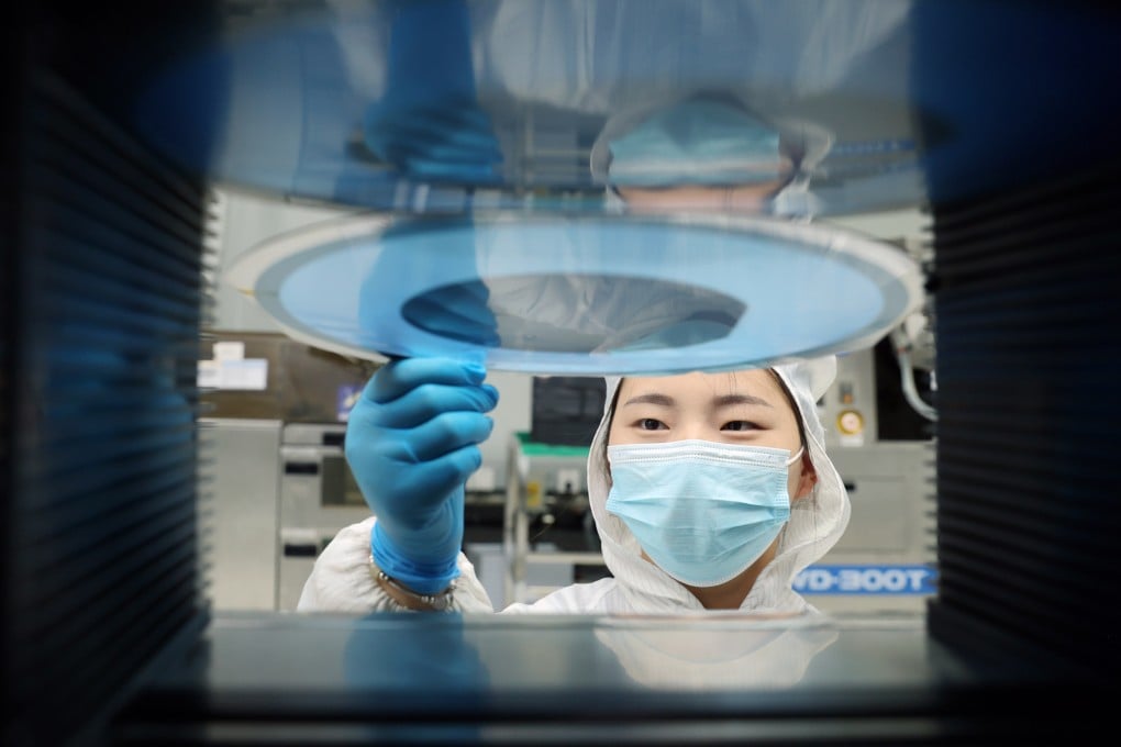
In a significant development for the semiconductor sector, a collaborative team of researchers from China has unveiled a groundbreaking method that can reduce defects in lithography—an essential phase in chip production—by as much as 99 percent. This remarkable achievement was made possible through the application of cryo-electron tomography (cryo-ET), which allowed the team to identify, for the first time, the tiny origins of prevalent manufacturing errors.
The study, which appeared in the journal Nature Communications on September 30, was led by Professor Peng Hailin from Peking University, in partnership with colleagues from Tsinghua University and the University of Hong Kong. Reviewers praised the innovation as a “fancy tool” that is expected to provide substantial benefits for both academic researchers and industry practitioners.
In an interview with Beijing-based Science and Technology Daily, Professor Peng elaborated on the implications of their findings, stating, “The team has proposed a solution compatible with existing semiconductor production lines.” He emphasized that this method could decrease lithography errors on 12-inch (30 cm) wafers by an impressive 99 percent, which could lead to significant cost savings in the market.
Lithography is a critical process in chip fabrication, akin to “printing circuits” onto semiconductor wafers such as silicon. Professor Peng described it as an ultra-precise “projector” that minimizes and transfers pre-designed circuit patterns onto a specialized film that coats the wafer, which is subsequently developed and fixed.


